- 您现在的位置:买卖IC网 > Sheet目录3382 > ISL28345FBZ-T13 (Intersil)IC OP AMP QUAD 1.2MHZ LN 14SOIC
ISL28325, ISL28345
4
September 27, 2011
FN7854.0
Absolute Maximum Ratings
Thermal Information
Maximum Supply Voltage . . . . . . . . . . . . . . . . . . . . . . . . . . . . . . . . . . . ....42V
Maximum Differential Input Current . . . . . . . . . . . . . . . . . . . . . . . . . . 20mA
Maximum Differential Input Voltage . . . . . . . . . . . . . . . . . . . . . . . . . . . . 42V
Min/Max Input Voltage . . . . . . . . . . . . . . . . . . . . . . . . V- - 0.5V to V+ + 0.5V
Max/Min Input current for Input Voltage >V+ or <V-. . . . . . . . . . . . . . . . ±20mA
Output Short-Circuit Duration (1 output at a time). . . . . . . . . . . . . . . . Indefinite
ESD Rating
Human Body Model . . . . . . . . . . . . . . . . . . . . . . . . . . . . . . . . . . . . . . . . 5kV
Machine Model . . . . . . . . . . . . . . . . . . . . . . . . . . . . . . . . . . . . . . . . . . . 300V
Charged Device Model . . . . . . . . . . . . . . . . . . . . . . . . . . . . . . . . . . . . . . 2kV
Thermal Resistance (Typical Notes 4, 5)
θJA (°C/W)
θJC (°C/W)
8 Ld SOIC. . . . . . . . . . . . . . . . . . . . . . . . . . . .
125
65
8 Ld MSOP. . . . . . . . . . . . . . . . . . . . . . . . . . .
160
55
14 Ld SOIC. . . . . . . . . . . . . . . . . . . . . . . . . . .
73
45
Maximum Storage Temperature Range . . . . . . . . . . . . . .-65°C to +150°C
Maximum Junction Temperature (TJMAX) . . . . . . . . . . . . . . . . . . . . .+150°C
Pb-Free Reflow Profile . . . . . . . . . . . . . . . . . . . . . . . . . . . . . . . see link below
http://www.intersil.com/pbfree/Pb-FreeReflow.asp
Recommended Operating Conditions
Ambient Temperature Range (TA) . . . . . . . . . . . . . . . . . . .-40°C to +125°C
CAUTION: Do not operate at or near the maximum ratings listed for extended periods of time. Exposure to such conditions may adversely impact product
reliability and result in failures not covered by warranty.
NOTES:
4.
θJA is measured with the component mounted on a high effective thermal conductivity test board in free air. See Tech Brief TB379 for details.
5. For
θJC, the “case temp” location is taken at the package top center.
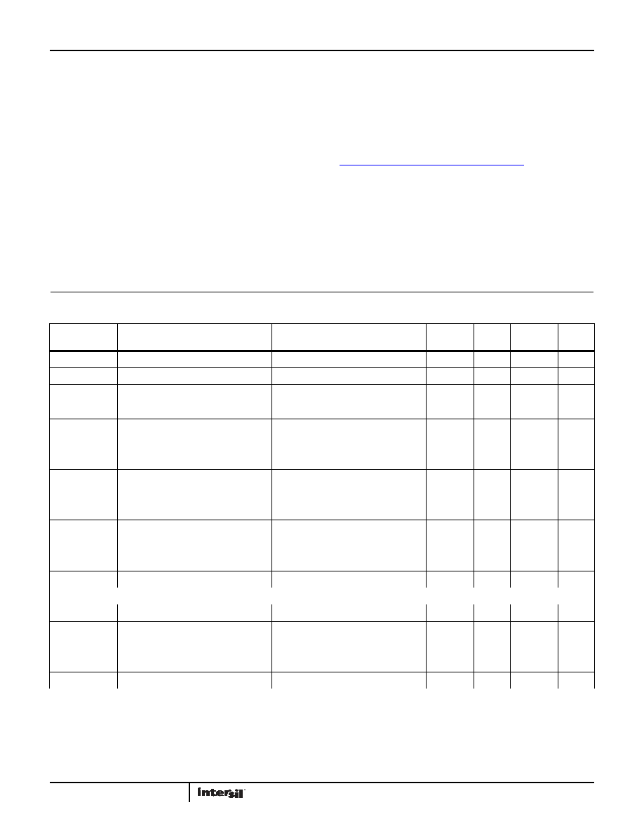
Electrical Specifications VS ± 5V and VS ± 15V, VCM = 0, VO = 0V, TA= +25°C, unless otherwise noted. Boldface limits apply over
the operating temperature range, -40°C to +125°C.
PARAMETER
DESCRIPTION
CONDITIONS
MIN
(Note 6)
TYP
MAX
(Note 6)
UNIT
VOS
Input Offset Voltage
-1
0.1
1
mV
TCVOS
Input VOS Temperature Coefficient
4
15
V/C
IB
Input Bias Current
-5
0.2
5
nA
IOS
Input Offset Current
-5
0.2
5
nA
VCM
Input Voltage Range
-13
13
V
CMRR
Common-Mode Rejection Ratio
VCM = -13V to +13V
80
100
dB
PSRR
Power Supply Rejection Ratio
VS = ±2.25V to ±20V
80
100
dB
AVOL
Open-Loop Gain
VO = -13V to +13V, RL =10kΩ to ground
100
110
dB
VOH
Output Voltage High
RL = 10kΩ to ground
13.0
13.5
V
VOL
Output Voltage Low
RL = 10kΩ to ground
-13.7
-13.5
V
IS
Supply Current/Amplifier
0.5
0.7
mA
0.9
mA
ISC
Short-Circuit
40
mA
VSUPPLY
Supply Voltage Range
± 2.25
± 20
V
AC SPECIFICATIONS
GBWP
Gain Bandwidth Product
AV = 1k, RL = 2kΩ
1.2
MHz
SR
Slew Rate, VOUT 20% to 80%
AV = 11, RL = 2kΩ, VO = 4VP-P
0.4
V/s
enVp-p
Voltage Noise VP-P
0.1Hz to 10Hz
0.4
VP-P
en
Voltage Noise Density
f = 1kHz
9
nV/
√Hz
in
Current Noise Density
f = 1kHz
0.1
pA/
√Hz
NOTE:
6. Compliance to datasheet limits is assured by one or more methods: production test, characterization and/or design.
发布紧急采购,3分钟左右您将得到回复。
相关PDF资料
SMCJ110CA
TVS BIDIRECT 1500W 110V SMC
77317-804-72LF
CONN HEADER .100 2ROW R/A 72POS
961228-5900-AR-PR
CONN HEADER R/A 28POS GOLD SMD
EL5165IWZ-T7
IC OPAMP CFB SGL 600MHZ SOT23-5
3431-2303
CONN HEADER 34POS STR LONG LATCH
108483078003049
CONNECTOR HEADER 78POS R/A
TLC2274INE4
IC OPAMP GP R-R 2.25MHZ 14DIP
EL5162ISZ-T7
IC AMP CFA SGL 500MHZ 8-SOIC
相关代理商/技术参数
ISL28345FBZ-T7
功能描述:IC OP AMP QUAD 1.2MHZ LN 14SOIC RoHS:是 类别:集成电路 (IC) >> Linear - Amplifiers - Instrumentation 系列:- 其它有关文件:TS1854A View All Specifications 标准包装:50 系列:- 放大器类型:通用 电路数:4 输出类型:满摆幅 转换速率:0.25 V/µs 增益带宽积:630kHz -3db带宽:- 电流 - 输入偏压:16nA 电压 - 输入偏移:1000µV 电流 - 电源:162µA 电流 - 输出 / 通道:48mA 电压 - 电源,单路/双路(±):1.8 V ~ 6 V 工作温度:-40°C ~ 125°C 安装类型:表面贴装 封装/外壳:14-SOIC(0.154",3.90mm 宽) 供应商设备封装:14-SO 包装:管件
ISL28345FBZ-T7A
功能描述:运算放大器 - 运放 ISL28345FBZ QUAD 40V PREC LW PWR OPERTNL RoHS:否 制造商:STMicroelectronics 通道数量:4 共模抑制比(最小值):63 dB 输入补偿电压:1 mV 输入偏流(最大值):10 pA 工作电源电压:2.7 V to 5.5 V 安装风格:SMD/SMT 封装 / 箱体:QFN-16 转换速度:0.89 V/us 关闭:No 输出电流:55 mA 最大工作温度:+ 125 C 封装:Reel
ISL28407
制造商:INTERSIL 制造商全称:Intersil Corporation 功能描述:Precision Single, Dual and Quad Low Noise Operational Amplifiers
ISL28407FBZ
功能描述:IC OPAMP PREC LN QUAD 14-SOIC RoHS:是 类别:集成电路 (IC) >> Linear - Amplifiers - Instrumentation 系列:- 标准包装:75 系列:MicroAmplifier™ 放大器类型:通用 电路数:1 输出类型:满摆幅 转换速率:0.03 V/µs 增益带宽积:100kHz -3db带宽:- 电流 - 输入偏压:1pA 电压 - 输入偏移:60µV 电流 - 电源:20µA 电流 - 输出 / 通道:5mA 电压 - 电源,单路/双路(±):2.3 V ~ 5.5 V 工作温度:-40°C ~ 85°C 安装类型:表面贴装 封装/外壳:8-SOIC(0.154",3.90mm 宽) 供应商设备封装:8-SOIC 包装:管件
ISL28407FBZ-T13
功能描述:IC OPAMP PREC LN QUAD 14-SOIC RoHS:是 类别:集成电路 (IC) >> Linear - Amplifiers - Instrumentation 系列:- 标准包装:75 系列:MicroAmplifier™ 放大器类型:通用 电路数:1 输出类型:满摆幅 转换速率:0.03 V/µs 增益带宽积:100kHz -3db带宽:- 电流 - 输入偏压:1pA 电压 - 输入偏移:60µV 电流 - 电源:20µA 电流 - 输出 / 通道:5mA 电压 - 电源,单路/双路(±):2.3 V ~ 5.5 V 工作温度:-40°C ~ 85°C 安装类型:表面贴装 封装/外壳:8-SOIC(0.154",3.90mm 宽) 供应商设备封装:8-SOIC 包装:管件
ISL28407FBZ-T7
功能描述:IC OPAMP PREC LN QUAD 14-SOIC RoHS:是 类别:集成电路 (IC) >> Linear - Amplifiers - Instrumentation 系列:- 标准包装:75 系列:MicroAmplifier™ 放大器类型:通用 电路数:1 输出类型:满摆幅 转换速率:0.03 V/µs 增益带宽积:100kHz -3db带宽:- 电流 - 输入偏压:1pA 电压 - 输入偏移:60µV 电流 - 电源:20µA 电流 - 输出 / 通道:5mA 电压 - 电源,单路/双路(±):2.3 V ~ 5.5 V 工作温度:-40°C ~ 85°C 安装类型:表面贴装 封装/外壳:8-SOIC(0.154",3.90mm 宽) 供应商设备封装:8-SOIC 包装:管件
ISL28407FBZ-T7A
功能描述:精密放大器 ISL28407FBZ QUAL PRC MICROPWR OPERTNL AM RoHS:否 制造商:Maxim Integrated 每芯片的通道数量: 输入补偿电压:0.25 mV at +/- 5 V 输入电压范围(最大值): 安装风格: 封装 / 箱体:SOIC-8 Narrow 封装:Tube
ISL28407FRZ
制造商:Intersil 功能描述:Wide Supply Range 4.5 ~ 40V , Precision Quad , Low Noise Operational Amplifiers .